
LAB FACILITIES
This Department has established well equipped and modern Physics, Chemistry & Language labs to upgrade basic technological skills of the first year students. The fundamental laboratories in the department are:
The Engineering Physics Laboratory:
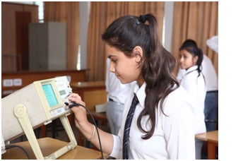 |
The Engineering Physics Laboratory is one of the major laboratories of the department. It enables the budding engineers to practically understand the fundamentals of the theory through a vast range of experiments. Experiments are conducted in the laboratory with the aim of making the budding engineers effectively use mathematical, scientific, and modern engineering tools in the practice of their professions. The lab is equipped with the latest equipment like laser units, facilities for measuring various properties of semiconductors like band gap, carrier density, and resistivity etc. |
Further, facilities are available for measuring optical fibre parameters like numerical aperture, attenuation etc. In the lab we also offer holographic studies. The basic focus in the Engineering Physics Laboratory is to develop scientific temper and encourage students to innovate in diverse technical areas for better understanding of technical and engineering problems. We believe that after conducting experiments under the able guidance of the faculty members, the students will have a sound theoretical and practical knowledge and they will be able to demonstrate the ability to identify, formulate and solve real-world technical problems.
Various Equipments of Engineering Physics Lab
 |
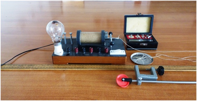
BASIC LASER KIT
This apparatus is used to measure the wavelength of visible light. It can also measure the spacing of grating. Specifications: Laser power: 5 mW Laser wavelength: 650 nm Gratings LPI: 12000
|
ELECTRICAL VIBRATOR
This apparatus is used to find the frequency of AC mains. This can also verify the law of vibrations of stretched strings.
Specifications:
Frequency of vibrator: 50 Hz
Field magnet strength: 100G
Rod material: Soft Iron
Linear mass density of thread: 0.0015 g/cm
TDIELECTRIC CONSTANT APPARATUS
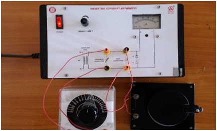
Specifications:
Radio frequency generator range:9-10MHz
Micro ammeter range: 0-50μA
Material of fixed capacitor: Aluminium.
Variable Gang Capacitor: 22-354pF
By using this apparatus, one can measure the dielectric constant and polarizability of a given dielectric slab.
STEWART & GEE’S APPARATUS
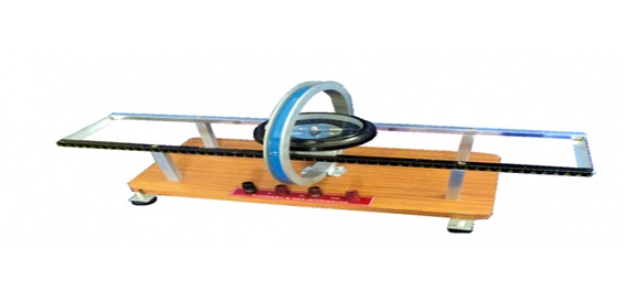
This apparatus is based on tangent law of magnetism, this apparatus is used to plot the variation of the magnetic field of the current carrying circular coil on the axis. It can also be used to verify Biot Sawart’s law.
Specifications:
No of turns of copper wire: 5, 50, 500
Size of copper wire: 24 SWG
OPTICAL FIBRE KIT
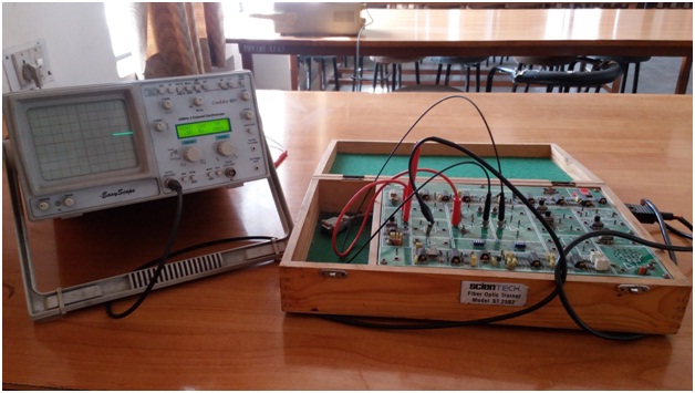
Using the optical fiber kit, one can measure NA and attenuation coefficient of the fiber. Bending loss can also be measured with the help of this kit.
Specifications:
Oscillator Frequency: 20 kHz
CRO: Dual channel 20 MHz
Fiber Type: Single Mode step index fiber
Fiber Length: 1m, 2m, 10m
Numerical aperture of fiber: 0.5
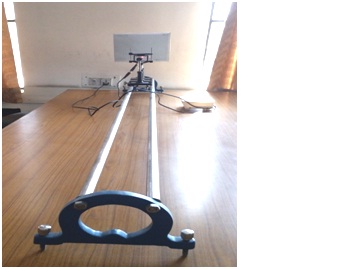
MICHELSON INTERFEROMETER
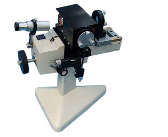 |
This apparatus can be used to find the wavelength of visible light. With this apparatus one can also determine the refractive index and thickness of transparent thin films. Specifications:
Least Count of main scale: 0.1 cm Least count of RMS : 0.001cm Least count of FMS: 0.00001cm Laser Wavelength: 650nm Laser Power Rating: 5mw
|
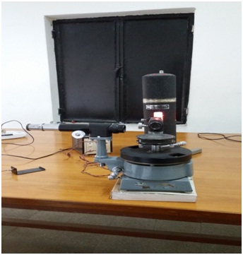
SPECTROMETER
| This apparatus can be used to
a) study the dispersion of light b) measure the refractive index of prisms and liquids. c) find angle of the prism d) angle of minimum deviation. e) find the value of Cauchy’s constants. Specifications:
Least count: 1/60o Wavelength of sodium vapour lamp: 5690Ao Power Rating of sodium vapour lamp: 200W Material of Prism: flint glass |
 |
The Engineering Chemistry Laboratory
 |
The Engineering Chemistry Laboratory has been designed to provide students with a basic understanding of the chemistry that may be required by engineers in the course of their careers. The Laboratory provides a broad range of Engineering Chemistry support services to the scientific and engineering programs at the institution and services of specialized analysis for government, academic, and industrial organizations. The Laboratory provides extensive facilities for thermodynamics, electrochemistry, polymers, corrosion, fuel combustion, water treatment and testing of environmental pollution–with emphasis on topics of interest in engineering. |
The Engineering Chemistry Laboratory has been designed to acquaint the students with practical knowledge of the basic phenomenon/concepts of chemistry that they face during course of their study in the industry and engineering field. The students will be able to understand and explain scientifically the various chemistry related problems in the industry/engineering and develop experimental skills for building technical competence. Also, students will be able to enhance the thinking capabilities in the modern trends in Engineering & Technology, learn and apply basic techniques used in chemistry laboratory for preparation, purification and identification. They learn to employ the basic techniques used in chemistry laboratory for analyses such as chromatography, spectroscopy, volumetric titrations, conductometry and stalagnometric method.The laboratory is equipped with Spectrometers, Conductivity meters, Colorimeters, pH meters, BOD Incubator, Flame photometers etc. to familiarise students with a variety of methods used to study matter from the molecular perspective. Various experiments cover the analysis of water (acidity, residual chlorine, hardness, BOD, COD measurements); spectroscopic studies of molecules; synthesis of organic polymers and chromatographic studies etc. In addition, further equipments and chemicals are available for the analysis of polluted water samples. The basic aim of the experiments conducted in the Laboratory is to train the students as both scientists and engineers in order to enhance their problem solving abilities and mould them into successful professionals and responsible citizens.
Various Equipments of Engineering Chemistry Laboratory:
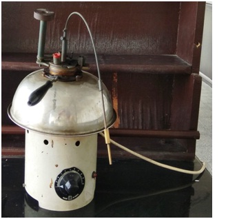 |
PENSKY MARTENS APPARATUS
This apparatus is used to measure flash point & fire point of lubricating oils, fuel oils, solvents, solvent containing material and suspension of solids. In the Pensky–Martens closed-cup flash-point test, a brass test cup is filled with a test specimen and fitted with a cover. The sample is heated and stirred at specified rates depending on the material that is being tested. An ignition source is directed into the cup at regular intervals with simultaneous interruption of stirring until a flash that spreads throughout the inside of the cup is seen. The corresponding temperature is its flash point. |
DIGITAL CONDUCTIVITY METER 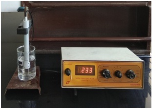
This meter is used to measure the ability of water-based solutions to carry electric current using probes to produce electrical voltage when placed into a solution
It is a convenient instrument for measurement of conductivity of various electrolytes such as caustic content of rinse water, Electrolytic impurities of Distilled/Demineralised water, Sulphuric acid, concentration in pickling baths, Anodizing tanks, Soil conductivity and other applications.
DIGITAL COLORIMETER
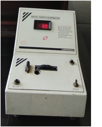
A colorimeter is a device used in colorimetry. In scientific fields the word generally refers to the device that measures the absorbance of particular wavelengths of light by a specific solution. This device is commonly used to determine the concentration of a known solute in a given solution by the application of the Beer-Lambert law, which states that the concentration of a solute is proportional to the absorbance. Digital colorimeters are widely used across different work areas including, environmental testing, clinical diagnostics, pharmaceutical analysis, and biochemistry. Besides being used for basic research in chemistry laboratories, colorimeters have many practical applications such as testing water quality by screening chemicals such as chlorine, fluoride, cyanide, dissolved oxygen, iron, molybdenum, zinc and hydrazine. They are also used to determine the concentrations of plant nutrients such as ammonia, nitrate and phosphorus in soil or hemoglobin in blood.
HOT AIR OVEN
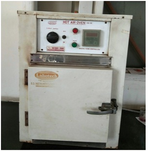
The electrical device which is widely used in medical products manufacturing industries, rubber industries, and many more to perform the process of sterilization using dry heat is known as Hot Air Oven. The instrument works on the basis of dry heat to sterilize the specimens and articles. The instrument can be operated at a temperature of 50° Celsius to 250° Celsius or 122° Fahrenheit to 482° Fahrenheit. The instruments are also known as the thermostat that controls the temperature. The device is provided with the digital panel to control the temperature digitally.
The device is equipped with the double-walled glass wool insulation that helps to conserve the energy to maintain the level of heat inside the cabinet as the inner layer of the cabinet is the less conductivity of heat energy whereas the outer layer is of metal. The instrument is widely used in pharmaceutical industries to sterilize the medical tools and instrument. It is a double walled chamber made up of stainless steel inside. The instrument works on the principle of fine gravity air convection in a highly heated electrical chamber of the unit. The instrument comprises of a double walled design and PID temp. Controller & automatically control units that helps to maintain the homogeneous temperature in the cabinet, return back to the preset temperature easily after opening the door of the hot air oven machine. It is a highly economical operation that offers simple operation of heating and drying of the common material. The instrument does not produce any kind of noises.
WATER DISTILLATION UNIT
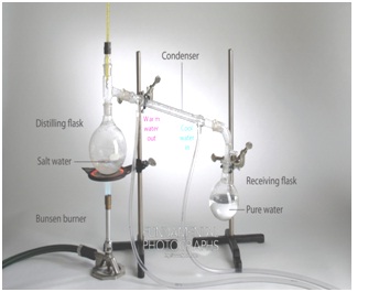
Glass Water distillation units produce highly treated and disinfected water for laboratory usage. The distillation process removes minerals and microbiological contaminants and can reduce levels of chemical contaminants.
Water distillers are neither intended to treat water that is visually contaminated nor intended to convert waste water to safe, microbiologically. A water distiller works by boiling water into water vapour, condensing it and then returning it to its liquid state. It is collected in a storage container.
Digital Language Lab (DLL)
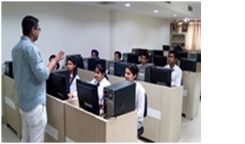 |
The Digital Language Laboratory which is situated in the newly built Knowledge Centre of the institute is our latest addition to the Department of Applied Sciences. It has been found that engineering students are proficient in their technical subjects but some of them are found wanting in the area of communication skills. So aiming to improve the proficiency of students in communication skills, the Digital Language Laboratory has been established. In today’s global scenario there is need to bring in innovations to train the students for improving their communication. | |||||||||||||||||||||||||||
|
The DLL Software is a pioneering, yet innovative solution that seamlessly integrates cutting-edge technology with internationally proven foreign language teaching and mastering methods to offer a fully computerized, modular and easy-to-use facility. We have replaced the traditional sound recording system in the language lab with this software. In Digital language laboratory we use software named Xclass which has a combination of pronunciation practice, video presentations, audio discussions and exercises. All this helps to create a genuinely interactive teaching and learning environment and thus language teaching and self directed language learning are done quite easily. In the Digital Language Laboratory the students learn all the nuances of English language effortlessly. So with improved communication skills, students have a better chance to get good packages and tackle the tough situations that they might face in their professional and personal lives Thus in the DLL the process of transformation of budding engineers into hard working professionals and responsible citizens begins. List Of Equipments Used In Language Lab
|
||||||||||||||||||||||||||||
Other facilities include a Spin Coater (Apex), Solvo thermal, Sol Gel and Co-precipitation Techniques, Electrochemical Cell for growth of Nanowires, Dual Source Meter (Keithley) for I-V Characteristics of fabricated Nano devices.
Achievements: Nano wires of copper (200nm) have been fabricated using electrochemical Cell and Templates synthesis techniques. Hetro-structure of Cu-Se and CdS Nano wires have been grown in the range of 10-200nm. Using chemical synthesis route we have prepared Nano particles and Nano rods Nano Needles of Barium Carbonate, Iron Oxolate, Ba Hexa-ferrites ,Zinc Oxide, Cadmium Oxide and Cadmium Sulphide .Nano particles of Zinc Oxide have been fabricated following Quenching Method with variation in time and temperature. The same composition has been prepared by Hydro Thermal Method also. SEM, TEM, XRD, UV- vis and FTIR characterization have been done for all these samples and reported in International journals of repute. The results of our investigation would certainly be helpful in the fields of Nano electronics, Opto electronics and Material science
Various Equipments of Nano-Technology Laboratory:
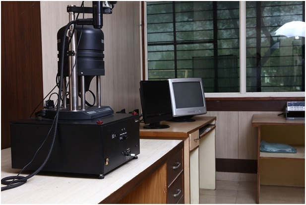
Atomic-force microscopy (AFM) or scanning-force microscopy (SFM) is a type of scanning probe microscopy (SPM), with demonstrated resolution on the order of fractions of a nanometer, more than 1000 times better than the optical diffraction limit. The information is gathered by “feeling” or “touching” the surface with a mechanical probe. Piezoelectric elements that facilitate tiny but accurate and precise movements on (electronic) command enable very precise scanning. The AFM has three major abilities: force measurement, imaging, and manipulation.
In force measurement, AFMs can be used to measure the forces between the probe and the sample as a function of their mutual separation. This can be applied to perform force spectroscopy.
For imaging, the reaction of the probe to the forces that the sample imposes on it can be used to form an image of the three-dimensional shape (topography) of a sample surface at a high resolution. This is achieved by raster scanning the position of the sample with respect to the tip and recording the height of the probe that corresponds to a constant probe-sample interaction (see section topographic imaging in AFM for more details). The surface topography is commonly displayed as a pseudo-colour plot.
In manipulation, the forces between tip and sample can also be used to change the properties of the sample in a controlled way. Examples of this include atomic manipulation, scanning probe lithography and local stimulation of cells.
Simultaneous with the acquisition of topographical images, other properties of the sample can be measured locally and displayed as an image, often with similarly high resolution. Examples of such properties are mechanical properties like stiffness or adhesion strength and electrical properties such as conductivity or surface potential. In fact, the majority of SPM techniques are extensions of AFM that use this modality.
The AFM has been applied to problems in a wide range of disciplines of the natural sciences, including solid-state physics, semiconductor science and technology, molecular engineering, polymer chemistry and physics, surface chemistry, molecular biology, cell biology and medicine.
Applications in the field of solid state physics include (a) the identification of atoms at a surface, (b) the evaluation of interactions between a specific atom and its neighbouring atoms, and (c) the study of changes in physical properties arising from changes in an atomic arrangement through atomic manipulation.
In cellular biology, AFM can be used to (a) attempt to distinguish cancer cells and normal cells based on a hardness of cells, and (b) to evaluate interactions between a specific cell and its neighbouring cells in a competitive culture system.
VACUUM COATING UNIT
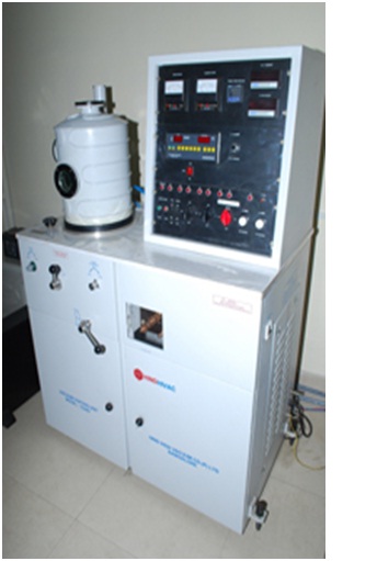 Vacuum coating and metalizing is the process of adding a thin film of aluminium or other coating to a material.
In principle, the process calls for the evaporation of the coating material inside a vacuum chamber, after which it condenses onto a web of substrate as it passes through.
Paper and film metalizing is utilized in the packaging and decorative market segments. The barrier and decorative markets are noted for their wide variety of products from beer labels to chip bags.
A thickness of less than one micrometer is generally called a thin film while a thickness greater than one micrometer is called a coating. It can be used in
- Electrical conduction: metallic films, transparent conductive oxides (TCO), superconducting films& coatings
- Semiconductordevices: semiconductor films, electrically insulating films.
- Optical films: anti-reflective coatings, optical filters
- Reflective coatings: mirrors, hot mirrors
- Tribologicalcoating: hard coatings, erosion resistant coatings, solid film lubricants
- Energy conservation& generation: low emissivity glass coatings, solar absorbing coatings, mirrors, solar thin film, photovoltaic cells, smart films
- Magnetic films: magnetic recording
- Diffusion barrier: gas permeation barriers, vapour permeation barriers, solid statediffusion barriers
- Corrosionprotection:
- Automotive applications: lamp reflectors and trim applications,Vinyl record pressing, manufacture of gold and platinum records.
SPIN COATER
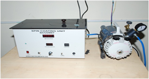
Spin coating is a procedure used to deposit uniform thin films to flat substrates. Usually a small amount ofcoating material is applied on the center of the substrate, which is either spinning at low speed or not spinning at all. The substrate is then rotated at high speed in order to spread the coating material by centrifugal force. A machine used for spin coating is called a spin coater, or simply spinner.
Rotation is continued while the fluid spins off the edges of the substrate, until the desired thickness of the film is achieved. The applied solvent is usually volatile, and simultaneously evaporates. So, the higher the angular speed of spinning, the thinner the film. The thickness of the film also depends on the viscosity and concentration of the solution and the solvent
Spin coating is used for many applications where relatively flat substrates or objects are coated with thin layers of material. The material to be made into the coating must be dissolved or dispersed into a solvent of some kind and this coating solution is then deposited onto the surface and spun-off to leave a uniform layer for subsequent processing stages and ultimate use.
Some technologies that depend heavily on high quality spin coated layers are:
- Photo resist for defining patterns in microcircuit fabrication.
- Dielectric/insulating layers for microcircuit fabrication – polymers, SOG, SiLK, etc.
- Magnetic disk coatings – magnetic particle suspensions, head lubricants, etc.
- Flat screen display coatings. – Antireflection coatings, conductive oxide, etc.
- Compact Disks – DVD, CD ROM, etc.